
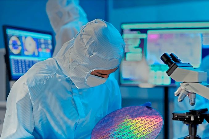
As a part of Samsung’s Q1 earnings announcement, the corporate has outlined a few of its foundry unit’s key plans for the remainder of the yr. The corporate has confirmed that it stays on monitor to assembly its purpose of beginning mass manufacturing of chips on its SF3 (3 nm-class, 2nd Era) know-how within the second half of the yr. In the meantime in June, Samsung Foundry will formally unveil its SF2 (2 nm-class) course of know-how, which can provide a mixture of efficiency and effectivity enhancements. Lastly, the corporate the corporate is making ready a variation of its 4 nm-class know-how for integration into stacked 3D designs.
SF2 To Be Unveiled In June
Samsung plans to reveal key particulars about its SF2 fabrication know-how on the VLSI Symposium 2024 on June 19. This would be the firm’s second main course of node based mostly upon gate-all-around (GAA) multi-bridge channel field-effect transistors (MBCFET). Enhancing over its predecessor, SF2 will function a ‘distinctive epitaxial and integration course of,’ which can give the method node increased efficiency and decrease leakage than conventional FinFET-based nodes (although Samsung is not disclosing the precise node they’re evaluating it to).
Samsung says that SF2 will increase efficiency of slender transistors by 29% for N-type and 46% for P-type, and huge transistors by 11% and 23% respectively. Furthermore, it reduces transistor world variation by 26% in comparison with FinFET know-how, and cuts product leakage by roughly 50%. This course of additionally units the stage for future developments in know-how by way of enhanced design know-how co-optimization (DTCO) collaboration with its prospects.
One factor that Samsung has not talked about in context of SF2 is bottom energy supply, so not less than for the second, there is no such thing as a indication that Samsung shall be adopting this next-gen energy routing function for SF2.
Samsung says that the design infrastructure for SF2 – the PDK, EDA instruments, and licensed IP – shall be finalized within the second quarter of 2024. As soon as this occurs, Samsung’s chip improvement companions will have the ability to start designing merchandise for this manufacturing node. In the meantime, Samsung is already working with Arm to co-optimize Arm’s Cortex cores for the SF2 course of.
SF3: On Monitor for 2H 2024
As the primary fab to introduce a GAAFET-based node, Samsung has been on the chopping fringe of chip development. On the similar time, nonetheless, that has additionally meant that they are the primary fab to come across and clear up the inevitable teething points that include such a significant transistor design change. Consequently, whereas Samsung’s first-generation SF3E course of know-how has been in manufacturing for rather less than two years now, the one publicly-disclosed chips made on the method to date have been comparatively small cryptocurrency mining chips – precisely the form of pipecleaner elements that do effectively on a brand new course of node.
However with that have in hand, Samsung is making ready to maneuver on to creating greater and higher chips with GAAFETs. As a part of their earnings bulletins, the corporate has confirmed that their up to date SF3 node, which was launched final yr, stays on schedule to enter manufacturing within the second half of 2024.
A extra mature product from the get-go, SF3 is being ready for use for constructing bigger processors, together with datacenter merchandise. In comparison with its direct predecessor, SF4, SF3 guarantees a 22% efficiency increase on the similar energy and transistor rely, or a 34% decrease energy on the similar frequency and complexity, in addition to a 21% logic space discount. Generally, Samsung pins quite a lot of hopes on this know-how, because it’s this technology of their 3nm-class know-how that’s poised to compete in opposition to TSMC’s N3B and N3E nodes.
SF4: Prepared for 3D Stacking
Lastly, Samsung can be making ready a variant of their last FinFET know-how node, SF4, to be used in 3D chiplet stacking. As transistor density enhancements have continued to sluggish, 3D chip stacking has emerged as a solution to maintain boosting general chip efficiency, particularly with trendy, multi-tile processor designs.
Particulars on this node are restricted, however it could appear that Samsung is making some modifications to account/optimize for utilizing SF4-fabbed chiplets in a 3D-stacked design, the place chips want to have the ability to talk each up and down. Based on the corporate’s Q1 monetary report, Samsung expects to finish their preparatory work on the chip-stacking SF4 variant in the course of the present quarter (Q2).
Sources: Samsung, Samsung